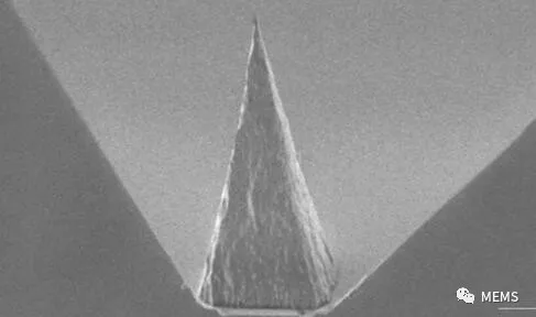
An example of a diamond pyramid tip used in the experiment, with a tip radius of approximately 10 nanometers, allowing sensing at nanoscale spatial resolution
According to the James Consulting, researchers at the Singapore Institute of Science and Technology (A*STAR) found that commercially available diamond tips used in atomic force microscopy (AFM) help make quantum nanosensing more cost-effective. Benefit and practicality.
The idea of ​​using a "color center", an optically active atomic defect in diamond as a probe, for performing highly sensitive nanoscale measurements such as electromagnetic fields, temperature or stress is well known. However, in practice, these experiments typically require expensive custom diamond nanostructures, and collecting weak optical signals generated by the color centers is also a challenge.
Now, Victor Leong, a colleague at the A*STAR Institute for Materials Research and Engineering, and the Institute of High Performance Computing recently published a study showing that the use of commercially available pyramidal diamond AFM tips with silicon vacancy centers may be helpful. This method has the following advantages.
First, the team's experiments using confocal microscopes and diamond tips arranged in different directions showed that the pyramid shape of the diamond tip acts as a weak infrared (738 nm) photoluminescence efficient collector generated by the color center. Due to the geometric effect, a larger portion of the emitted photoluminescence is directed to the bottom of the pyramid, resulting in a signal that is eight times stronger in this direction than in the other directions. In the experiment, the bottom of the tip was attached to a silicon nitride cantilever beam and was transparent to infrared light, enabling photoluminescence to pass through and be collected by a spectrophotometer.
Leong explains, “In many nanosensing applications, the weak signal itself will fundamentally limit sensitivity. The ability to collect and detect larger signals improves many performance metrics such as minimum detectable signal, resolution, and measurement time. ""
Second, these diamond tips are commercially available and compatible with AFM and microscope equipment, providing a practically implementable approach. Leong commented, “These ready-made diamond AFM tips are easy to obtain and inexpensive. Each sells for about S$100. If they contain color centers with suitable optical properties, they will likely be a low-cost alternative to other diamond nanoprobes. Low cost and ease of use help to promote the rapid development and adoption of quantum technology applications."
Very small diamond tips with a radius of about 10 nanometers and a length of about 15 microns mean that they can be very close to the sample to be studied, maximizing measurement sensitivity and spatial resolution. Leong commented, “These diamond tips can be used for challenging sensing applications compared to other diamond structures, such as drawing the electromagnetic properties of deep trenches or closely surrounding nanostructures.â€
To date, the team has been working on diamond tip with silicon vacancy color centers, but Leong said it is also possible to introduce nitrogen vacancy centers that are common in magnetic measurement studies. Leong explained, “The batch of diamond tips mentioned in the paper is manufactured in a nominally nitrogen-free process, so there are many silicon vacancy centers, and there are very few nitrogen vacancy centers. However, we have obtained other separate batches of diamond tips. Contains a high concentration of nitrogen vacancy centers."
Now that the team has proven that it is feasible to increase optical readings from the diamond tip, the next phase of the study will optimize performance and perform some practical sensing experiments. “We plan to deploy these tips in real-world nanosensing applications,†Leong said. “The current vision includes nanoscale magnetic sensing and surface research.â€
Stevia Rm,Stevia Rebaudioside M,Stevia Reb-M,Rebaudioside M
JINING USP INTERNATIONAL CO.,LTD. , https://www.uspintl.com